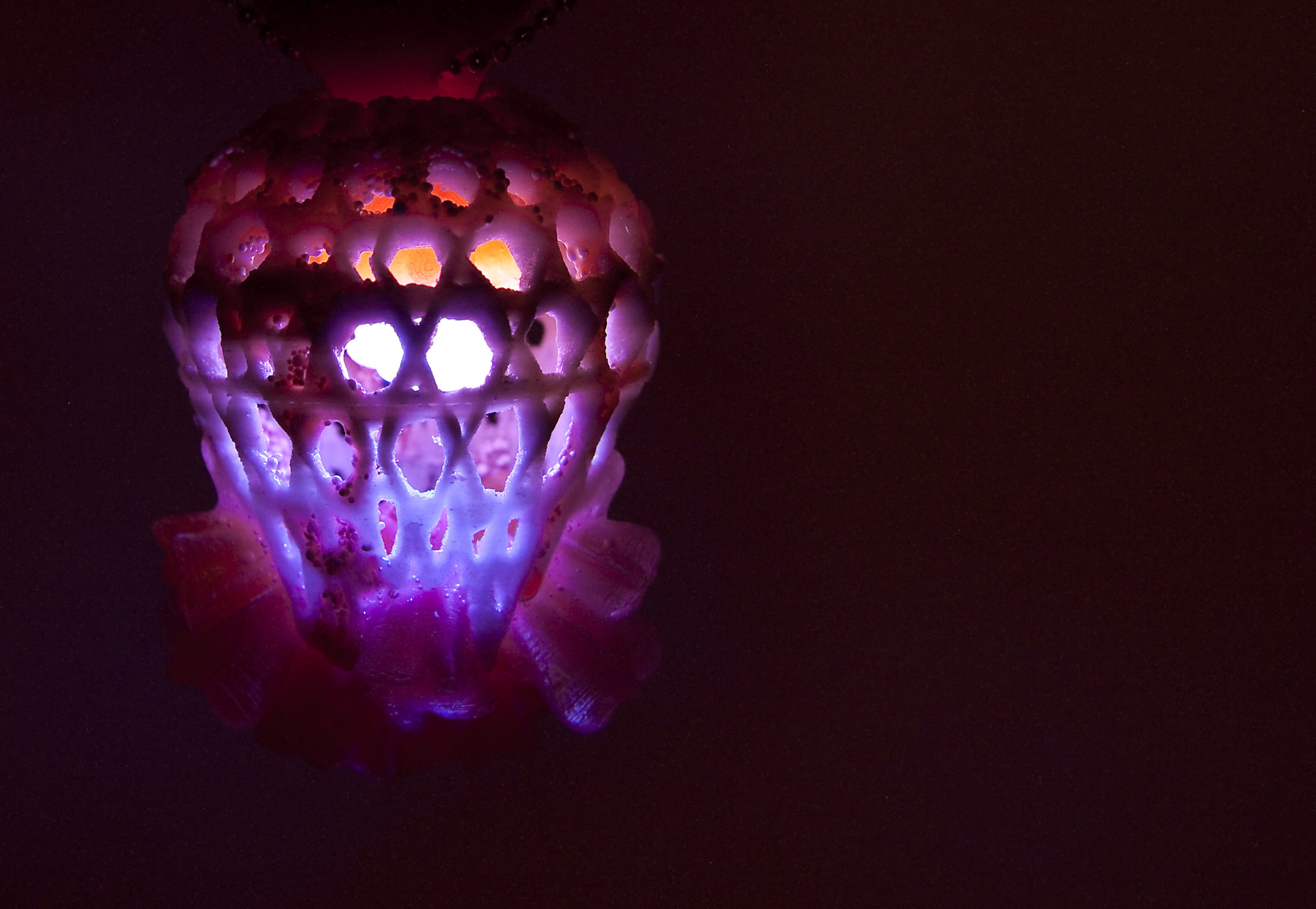
Sometimes, having trained as a jeweller is surprisingly useful when it comes to working with electronics. After finally having got my head round the way in which ICs are programmed and used on circuit boards with this handy programmer, I decided that the easiest way to incorporate small-scale electronic components in my jewellery was to make a customised PCB (Printed Circuit Board) – it was time to put the theory into action! Not only would creating custom PCBs save me a whole lot of cash (the components are a fraction of the price of a finished circuit board), but it would also allow me to fully control the shape and size of my PCBs.
The first step in this endeavour was creating the circuit design files. Now, there are a number of ways to do this, and which method you use depends largely on your skill base, the complexity of the circuit you want to design and what method you will be using to produce the final board. There are a lot of great freeware packages available online, the most popular probably being the EAGLE PCB software offered by cadsoft. However, I could not get the freeware version to install on my system, and so decided to look for alternatives in the meantime. Fritzing offers a PCB generator as part of its package, but I wanted to use a software that would let me customise tracks and components easily, while offering a library of ‘pre-fab’ parts to play with until I am more familiar with the pin spacing of components and minimum track widths, so after a false start with the very basic FreePCB, in the end I chose the DesignSpark PCB package (v.7.1). Equipped with a full library of parts, as well as a searchable online database of parts offered by UK electronics distributor RS components, this program was really easy to use and before long I had laid down my first PCB design. For the experts out there it is also possible to make PCB layouts in any vector-based graphics software (such as Adobe Illustrator), but of course you will have to be 100% certain of your design as there are no automatic checks or set design rules in a graphics application. DesignSpark has customisable rules and warns you if components are spaced too closely together or if there are missed connections. It is by no means perfect, and I ended up tweaking some of my PCB designs in Illustrator after finalising the layout in DesignSpark to account for crooked or awkward tracks, as well as adding my logos to the boards.
Once I was happy with my designs, I tried to figure out which would be the best way to get them onto the copper covered particle board. After initially considering using the iModela at our MakeSpace, I decided that maybe the old ways are the best and ordered the chemicals required for photoetching. From my time as an undergraduate at ECA I still had some PNP blue resist lying around the studio, and even though some people swear by the slightly more accurate UV-exposure method for transferring your artwork to the resist, if you have a laser printer at home the PNP is easily the most hassle-free solution. After transferring your design to the dull side of the film with a laser printer or photocopier, the film is ironed onto the thoroughly cleaned and de-greased surface of your PCB board. When ironing on the resist, don’t put too much pressure on the iron, as it can spread the ink and make your tracks bleed into each other. There are some great tutorials online about this process, although I would recommend the use of a glassfibre brush (available from enamelling suppliers) for degreasing your board rather than acetone, as it is more reliable and there’s no need for chemicals.
Once you have transferred your artwork to the board, gently peel off the PNP film, and touch up any imperfections or gaps with a black indelible marker pen. In order to preserve the rest of your board, mask off any areas that are not to be etched with brown parcel tape. You should end up with something like this:

The shiny exposed copper areas are going to be etched away, leaving only the black track marks behind. Depending on which chemical you use, prepare as stated on the packaging and fill a small plastic tub with just enough solution to cover your particle board. Gently slide in your board, and agitate the solution roughly every two minutes either with a feather or by gently tipping the tub from side to side. Eventually, all the copper will have been eaten away by the acid, at which point the board needs to be removed quickly from the acid bath with plastic tweezers and rinsed thoroughly under running water. Don’t ever leave your board unattended in the acid, as the acid can undercut the tracks if left too long. Some people have also successfully used the sponge etching method, but I prefer the traditional way as you have a lot less direct contact with the chemicals. After the board has been thoroughly rinsed, you can remove the parcel tape and the resist with acetone.The end result will look similar to this:
 See how to finish the job in part II…